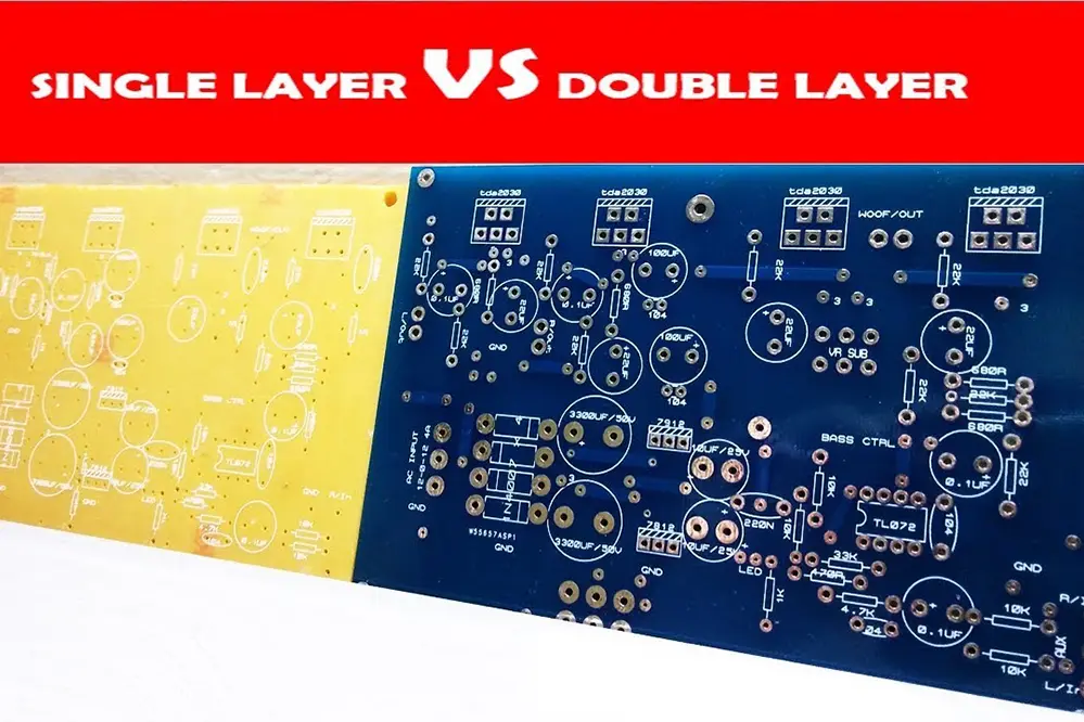
What is the difference between double layer PCB and single layer PCB of LED strip? This question often puzzles both novices and experts in the field of LED lighting. Many assume that all PCBs are created equal, leading to common misconceptions that can hinder the performance of LED projects. Understanding these differences is crucial for anyone looking to optimize their lighting solutions.
The choice between single and double layer PCBs can significantly impact the efficiency, durability, and cost-effectiveness of LED strips. Double layer PCBs offer enhanced electrical performance and greater design flexibility, making them ideal for complex applications. On the other hand, single layer PCBs are often more cost-effective and easier to manufacture, suitable for simpler projects.
Ready to illuminate your knowledge? Dive into the details and discover how the right PCB choice can transform your LED lighting experience.
Introduction to PCB Layers in LED Strips

In the world of LED strips, printed circuit boards (PCBs) serve as the backbone of innovation and technology, steering their performance and application potential.
In essence, PCBs are the crucial platforms upon which LED strips are constructed, with each layer of the PCB playing a vital role in determining the overall performance of the device. Single-layer PCBs consist of just one conductive layer, often making them suitable for standard, less complex applications. Such simplicity provides cost advantages and easier manufacturing processes, making them accessible for basic LED strip uses.
Conversely, double-layer PCBs feature two conductive layers, amplifying their capacity to handle more intricate circuitry. This expanded design capability ensures that more complicated and sophisticated LED configurations can be accommodated, facilitating enhanced electrical performance and functionality.
Ultimately, understanding PCB layers, including the role of circuit density, is key to unlocking the true potential of LED strips. By delving into the benefits and appropriate uses of single and double-layer PCBs, individuals can ensure they select the most suitable option for their specific needs and applications. This knowledge empowers both hobbyists and professionals to harness LED technology effectively, pushing the boundaries of what’s possible in lighting solutions and beyond.
What is a Single Layer PCB?
A single-layer PCB comprises a singular conductive layer.
This basic construction means that all electronic components and conductive paths are consolidated onto one side of the board. The simplified layout not only results in reduced manufacturing costs but also eases the production process, making these PCBs particularly favorable for straightforward applications. Consequently, they are an ideal choice for uncomplicated LED strip projects.
Their simplicity is their most defining characteristic.
Single-layer PCBs are integral to projects where one-sided conductivity suffices—like in many standard LED strips—due to their straightforward design and reliable performance.
By selecting single-layer PCBs for appropriate projects, developers can achieve efficient solutions that align technical needs with economic viability. With advancements in technology continually enhancing their utility, single-layer PCBs remain a vital, cost-effective tool in the modern engineer’s arsenal. This dynamic ensures even basic lighting applications can achieve contemporary relevance with streamlined, yet impactful, execution.
Design and Structure of Single Layer PCBs
Single-layer PCBs represent the most fundamental type of printed circuit board, crafted with conductive pathways situated only on one side.
These pathways, critical for transmitting electrical signals within a simplified circuit structure, are vital for foundational electronic designs. The board comprises a substrate, often FR4 or similar insulating materials, providing stability and insulation. A copper layer runs above the substrate, forming the requisite circuit configuration for power distribution. This streamlined configuration captures the essence of minimalism, allowing for cost-effective production while maintaining consistent functionality.
In essence, this architecture serves as a convenient blueprint for numerous LED strip applications. With the insulating substrate providing the base and a layer of conductive copper overlaid, these boards efficiently manage electrical currents with robustness and reliability across straightforward applications.
The design simplicity of single-layer PCBs directly translates into ease of manufacture and lower costs, enticing designers seeking uncomplicated yet efficient electronic solutions. As the backbone of many cost-effective projects, these PCBs exemplify an elegant harmony between simplicity and capability, ensuring any project harnessing their power can achieve technological and economical balance. Their enduring design principles reaffirm their relevancy in a consistently evolving technological landscape.
Advantages of Single Layer PCBs
Single Layer PCBs stand as a testament to simplicity, offering designers a straightforward approach that emphasizes reliability, accessibility, and cost-effectiveness essential for numerous LED strip applications.
One significant advantage is the reduced complexity in manufacturing, which results in lower production costs.
Moreover, these PCBs simplify the design process, avoiding the complications that often come with multilayer boards.
Such simplicity also facilitates easier troubleshooting during maintenance, promoting longevity and durability in various projects.
These features position Single Layer PCBs as an ideal choice for projects operating within tight-budget constraints, allowing innovators to allocate resources toward other aspects of development while maintaining functionality.
Tailoring to straightforward specifications yet robust enough to perform under diverse conditions, Single Layer PCBs provide an empowering foundation for creating sustainable, impactful LED solutions.
Limitations of Single Layer PCBs
Restricted in handling complex, multi-function electronic circuits.
While Single Layer PCBs are cost-effective, they can fall short in advanced applications. The lack of additional layers limits their capacity to support more intricate systems, which can stymie integration of sophisticated components or circuits that demand higher connectivity. Consequently, their use in high-performance or densely packed applications can be quite constrained.
This restriction confines them to simpler, less powerful designs.
When there is a necessity to accommodate more – in terms of both space and components – the single-layer design can pose significant challenges in maintaining efficiency and capability.
Faced with the evolving technological landscape and ever-increasing demand for compact and powerful electronic solutions, foreseeing these limitations is crucial for innovative growth. Single Layer PCBs, while invaluable in many contexts, must eventually yield to advanced multi-layer alternatives to embrace the full potential of modern technology developments.
What is a Double Layer PCB?
A double layer PCB, sometimes called a two-layer board, is a marvel epitomizing the best of multi-layer configurations, offering a substantial leap beyond its single-layer counterpart.
These configurations expand into the third and fourth dimensions.
Essentially, double layer PCBs feature an additional layer of conductive material, producing more versatile (albeit slightly more complex) circuit layouts.
This additional layer can accommodate enhanced connectivity in intricate designs, empowering more sophisticated electronic advancements.
Such structures enable the creative mounting of LED strips in channels or patterns that a single layer might struggle to maintain, providing manufacturers with unique design possibilities along with efficiency.
Ultimately, the rise of these boards means it’s easier to achieve innovation. Double layer PCBs pave the way for unparalleled creativity in the electrical arena.
Design and Structure of Double Layer PCBs
Double layer PCBs introduce a transformative leap in circuit design, enhancing both complexity and capability through the use of vias. In essence, they unlock a plethora of possibilities for intricate electrical schematics and advanced connectivity solutions, especially in LED lighting systems that demand a high level of precision and reliability.
The design of a double layer PCB comprises two layers of copper foil, separated by an insulating substrate. This construction allows for denser and more intricate routing paths, as each layer can play a distinct role in the circuit’s functionality. This dual-layer approach enables complex signal routing while minimizing interference, a critical factor in high-performance LED applications.
Moreover, double layer PCBs accommodate a greater number of components due to increased surface area without sacrificing compactness. For LED strips, this means not only can more LEDs be connected, but they can be organized to create more dynamic lighting patterns, enhancing both aesthetic and performance parameters.
Consequently, double layer PCBs present an innovative platform for those looking to push the boundaries of LED technology. Engineers and designers benefit from the flexibility and performance enhancements these boards offer, which allow for more intricate list circuit paths, reducing cross-talk and electromagnetic interference. These advancements therefore translate into superior product performance, solidifying their status as a game-changer in PCB design.
Advantages of Double Layer PCBs
Double layer PCBs boost LED strip efficiency.
By utilizing two conductive layers, these PCBs provide enhanced functionality. This increase in layers allows for more intricate circuit designs, which can help LED strips achieve higher performance levels. Additionally, having two layers helps in optimizing the layout to reduce electromagnetic interference, a common issue in densely packed electronic environments.
The increased complexity enhances creative design.
Enhanced designs lead to greater resilience against – and thereby less chance for – system failures by providing alternative routing paths in case of unanticipated interruptions, ensuring continued operation without compromising performance.
Furthermore, double layer configurations empower innovative developers by unlocking boundless possibilities for expanding the capabilities of LED strip technology beyond conventional applications. With this technology, designers can introduce a higher level of creativity to their projects, even envisioning concepts for the next generation of lighting solutions.
Limitations of Double Layer PCBs
While double layer PCBs offer numerous advantages, they are not without their constraints, particularly in the realm of LED strip applications. These boards can present challenges both in design complexity and manufacturing costs.
One primary limitation is the increased fabrication complexity. Double layer PCBs require more intricate processing steps.
Additionally, they demand precise alignment and higher precision, which inherently lead to higher production costs—factors crucial for cost-sensitive LED strip markets.
This complexity also extends to the design and testing phases, necessitating specialized design software and skilled professionals to ensure accurate functionality and performance.
Furthermore, the sheer density of routing paths can sometimes result in signal integrity issues, requiring meticulous attention to detail in the layout process to maintain optimal operation and prevent interference.
Ultimately, the trade-off for the expanded capabilities offered by double layer PCBs provides an opportunity for further innovation, yet it is crucial to balance this with the nuanced challenges they bring to the design and manufacturing process.
Key Differences Between Single and Double Layer PCBs

Single-sided PCBs, often considered the fundamental backbone, boast a simple construction with components on one side. This straightforward design allows wide accessibility, making them a cost-effective and efficient choice for straightforward applications like basic LED strips.
Conversely, double-layer PCBs offer a “dual side” advantage. These allow for a denser arrangement of components, thus accommodating more complex circuit designs. As a result, the versatility of the double-layer setup provides enhanced routing capabilities, which are particularly advantageous in more sophisticated LED lighting strips demanding higher functionality and power management levels.
Material Usage and Cost
In the realm of PCBs, single-layer boards utilize fewer materials, contributing to cost efficiency. These simpler designs typically require less copper and fewer production steps.
Double-layer PCBs, with added complexity, employ more materials like extra copper layers. This necessity for enhanced material usage translates to higher manufacturing expenses, reflecting their advanced capabilities.
Double-layer designs employ 50% more material, enhancing robustness but at a higher cost.
Ultimately, if budget constraints dictate your choices, the simplicity of single-layer PCBs offers savings. However, it is crucial to remember that investing in double-layer PCBs can yield significant advancements in performance that may outweigh the initial costs in sophisticated LED strip designs. The decision hinges on weighing up-front costs against long-term benefits.
Electrical Performance and Conductivity
When considering electrical performance, double-layer PCBs often surpass single-layer alternatives due to their enhanced complexity and design capabilities.
- Improved Conductivity: Double-layer PCBs allow traces on both sides, reducing resistance and enhancing current flow.
- Signal Integrity: More layers support better signal integrity, minimizing interference and maintaining signal clarity.
- Heat Management: Offers better heat dissipation, essential for high-power applications.
- Design Flexibility: Double layers allow for complex, space-saving designs crucial for advanced LED strips.
Single-layer PCBs may offer sufficient conductivity for basic applications but lack the robust features of double-layer designs.
The layered structure of double-layer PCBs supports superior electrical performance, significantly impacting LED strip efficacy in dynamic environments.
Heat Dissipation and Thermal Management
Heat dissipation plays a pivotal role in the functionality of LED strips, impacting the lifespan and reliability.
Double-layer PCBs offer improved thermal management due to their ability to distribute heat more evenly. The presence of additional layers facilitates efficient heat flow away from critical components. This results in better thermal conductivity, crucial for maintaining optimal operating temperatures.
Conversely, single-layer PCBs often struggle with heat dispersion, making them less suitable for high-intensity applications. The limited surface area restricts heat dissipation, potentially leading to overheating and reduced performance longevity. Effective heat management ensures that LED strips operate efficiently, even in demanding conditions.
Ultimately, the choice between single and double-layer PCBs depends on the thermal requirements of your LED application. Opting for a double-layer PCB may justify the additional investment by offering superior thermal regulation.
Making well-informed decisions on PCB selection can enhance the performance and durability of your LED systems.
Flexibility in Design and Applications
The distinction between single and double-layer PCBs plays a pivotal role in design flexibility, significantly affecting an LED strip’s adaptability across various applications.
Double-layer PCBs open doors to more intricate electronic configurations.
Notably, multilayer designs cater to sophisticated circuit requirements, allowing for (often indispensable) higher levels of customization and versatility.
Their ability to interweave connections across layers provides unparalleled adaptability and increased functionality.
Single-layer PCBs, despite their simplicity, excel in straightforward applications, offering ease of manufacturing and cost efficiency, a point of attraction for standard lighting solutions where complexity is less demanded.
Thus, the spectrum of PCB layering offers a tailored match for anyone’s need to maximize design potential. Multilayer configurations kindle boundless creative possibilities and elevate technological advancements.
Durability and Reliability
The durability and reliability of PCBs are crucial aspects influencing the performance of LED strips.
Double-layer PCBs offer a robustness that is a testament to their complex design, which intrinsically supports greater resilience. The dual layers provide a backup system, ensuring continuity of function even if one layer encounters a fault. As a result, these PCBs are often favored for demanding environments requiring enhanced reliability.
Conversely, single-layer PCBs, while simpler, still provide a trusted solution for less demanding applications. Their lack of complexity can be an advantage, reducing potential failure points and ensuring that the PCB performs consistently under stable conditions.
In conclusion, both single and double-layer PCBs offer distinct advantages in terms of durability and reliability, each tailored to specific needs and environments. Double-layer constructs are ideal for scenarios demanding intricate reliability, while single-layer PCBs remain steadfast champions of durability in standard uses. Such versatility ensures that every application can access the ideal balance of strength and reliability.
Applications of Single Layer PCBs in LED Strips

Single-layer PCBs have proven indispensable for the efficient functioning of LED strips, offering steadfast reliability at a cost-effective price point. These PCBs are a crucial element when simplicity is key.
Ideal for applications where robust, uncomplicated circuits can deliver desired outcomes. These boards excel in environments where the complexity of a double-layer PCB is unnecessary.
Their usage extends to decorative lighting, where uniform illumination without intricate control is needed, thus serving as a backbone for creative lighting projects that require steady performance and reliability.
The intrinsic benefits of single-layer PCBs make them a go-to choice in a plethora of LED strip applications. Their straightforward design allows for quick manufacturing and assembly processes, thus speeding up project timelines and reducing costs. In essence, single-layer PCBs embody “less is more” by delivering simplicity without compromising on performance.
Applications of Double Layer PCBs in LED Strips
Double-sided layer PCBs unlock greater functionality and adaptability for LED strip applications that demand complexity.
In recent years, industry innovation led to double layer PCB designs for LED strips that require improved thermal management and increased electrical performance. These designs cater to scenarios that benefit from having more intricate circuits and flexible configurations.
As technology progresses, there is an ever-increasing demand for products that can integrate a multitude of functions without compromising on space. Double layer PCBs help meet this need by providing room for additional components and circuitry essential for addressing sophisticated lighting solutions.
Particularly within the realm of LED strips, double layer PCBs are pivotal for applications featuring dynamic color changes, advanced dimming capabilities, and intricate control mechanisms. They empower creative installations where precision and versatility are paramount, such as in architectural lighting and elaborate displays.
The potential for customization with double layer PCBs is virtually limitless. Their ability to host complex designs ensures they meet the rigorous requirements of high-performance LED strip installations.
Considerations for Choosing Between Single and Double Layer PCBs
When deciding between single and double layer PCBs for LED strips, assessing your specific project requirements is vital.
In recent years, notable technologists, including a leading design thought leader, pointed out that the choice often hinges on factors like cost-effectiveness, design complexity, and the level of performance desired. This requires evaluating the trade-offs.
Additionally, it’s not just about cost; there’s also an opportunity to address a strategic balance between simplicity versus the intricate needs of your application. Double layer PCBs, for example, are excellent for complex light shows.
Consider the scale of the project too. Single layer PCBs, which fit well in simpler settings, might not handle the load for high dynamic color changes and advanced functionalities, which double layer PCBs excel in.
Ultimately, carefully weighing these factors will ensure the selected PCB meets your LED strip project’s requirements optimally.
Conclusion and Recommendations
Understanding the difference between double layer and single layer PCBs for LED strips is crucial for optimizing lighting solutions. Many people mistakenly believe that all PCBs are the same, which can lead to suboptimal performance in LED projects.
Double layer PCBs offer enhanced electrical performance and greater design flexibility, making them ideal for complex applications. In contrast, single layer PCBs are more cost-effective and easier to manufacture, suitable for simpler projects that don’t require advanced features.
Choosing the right PCB can significantly impact the efficiency, durability, and overall success of LED systems. By making informed decisions, you can enhance the quality and performance of your lighting solutions.


